Just beta-tested @reactorworld LingBot inside my Omnia 3D — World Editor and it’s wild.! https://t.co/xC6YeW8skt
Navigate a live AI world with WASD + mouse drag, grab a frame → paint in Sketch → push it back as the new reference and keep going. @taiuti
Almost like painting directly into the stream in real time.
more to come!. @reactorworld
#Omnia3D #Reactor #LingBot #AIvideo #creativeAI #worldbuilding #gamedev #realtime
🔥 #ICRA2026 Best Paper Finalist
The era of "robot VLA = single-arm gripper" is ending.
Introducing Dexora — the first open-source Vision-Language-Action system for dual-arm, dual-hand, 36-DoF dexterous manipulation.
🦾 Dual Arms
🖐️ Dual Hands
🎯 36 DoF Control
🌍 Open Source
Trained on:
• 100K simulated trajectories
• 10K real-world demonstrations
Dexora achieves:
✓ 90%+ success on basic manipulation
✓ Strong dexterous manipulation performance
✓ Cross-embodiment generalization
Our key hypothesis:
Train on the hardest embodiment. Transfer to simpler robots later.
Instead of scaling up gripper policies, we train directly in the most expressive action space and project downward to simpler embodiments.
This may be a practical path toward universal robot controllers.
🎥 Demos: https://t.co/Qkvzl8d5Dl
📄 Paper: https://t.co/InWVHE9k8S
Can AI design real engineering parts? 🛠️
Watch CadXStudio generate a production-ready 6M switch board assembly with 1.5° draft angles & perfect snap-fits. Engineering, not shapes.
Full video: [https://t.co/SaRkrXrruU]
Try the engine for $2: [https://t.co/uhtHLA2YNY]
Researchers report the electrochemical control of chirality in layered semiconductor materials. By reversibly inserting and removing chiral molecules, they successfully demonstrated switching of chirality in the semiconductor and control of the spin direction of electrons flowing through it, opening up possibilities for chiral spintronics and next‑generation electronic devices. https://t.co/4pqF4E9XEm
TIMECLAW wraps a small LLM in a numeric runtime, lets it create its own tools, and outperforms 235B-parameter models on contextual time-series tasks. The ablation table alone proves the claim.
https://t.co/feDVicYuXX
🧵 Today we're sharing a deep dive into Huawei's ‘Tao (τ) Law’, written by 乱序摸鱼, a Huawei HiSilicon chip architect.
As traditional scaling becomes increasingly difficult, the semiconductor industry is searching for the next growth curve.
Huawei's proposal is both ambitious and practical:
Use 3D integration not just as a packaging technology, but as a new design paradigm for future mobile SoCs.
This isn't simply about stacking more silicon.
It's about turning 3D space into a first-class design dimension for architecture, packaging, thermals, power delivery, and even OS scheduling.
The article explores a bigger question: What comes after conventional transistor scaling?
Let's dive in 👇
1️⃣ Why Mobile Chips Need A New Direction
Mobile devices want everything at once:
• more AI
• bigger batteries
• better cameras
• higher performance
• lower power
But motherboard space isn't growing.
Meanwhile, traditional 2D scaling is becoming increasingly expensive, both economically and physically.
The next frontier may not be smaller transistors alone.
It may be learning how to build upward.
🏗️ In other words, future gains may come from architectural density, not just transistor density.
2️⃣ Huawei Didn't Invent 3D ICs
The industry has been exploring 3D integration for years:
• AMD's 3D V-Cache
• Intel Foveros
• TSMC SoIC
• Apple's UltraFusion
The real question isn't: "Can chips be stacked?"
It's - "Can core logic itself be folded across multiple layers?"
That's a much harder problem.
Most existing solutions focus on:
• cache stacking
• chiplet integration
• package-level interconnects
Huawei's discussion goes further:
⚡ Can CPU, GPU, NPU and cache structures themselves be partitioned across multiple silicon layers?
3️⃣ Why Wafer-to-Wafer Matters
Huawei's proposed direction isn't traditional chiplets.
It's wafer-to-wafer face-to-face bonding.
Why?
Because logic folding requires extremely dense vertical interconnects.
The goal isn't modularity, but making two logic layers behave like one piece of silicon.
🔬 Compared with conventional packaging approaches, wafer-level hybrid bonding can dramatically reduce:
• interconnect length
• latency
• energy per bit transferred
Those benefits become critical once logic starts spanning multiple dies.
4️⃣ Why 1.5μm Pitch Matters
Pitch determines how many vertical connections can fit into a given area.
Smaller pitch means:
✅ higher bandwidth
✅ shorter signal paths
✅ lower communication energy
❌ lower yield
❌ harder manufacturing
❌ tighter process control requirements
The article argues that 1.5μm hybrid-bonding pitch is aggressive enough to enable meaningful logic folding, while remaining manufacturable at scale.
📈 At this density, vertical connectivity begins approaching the scale needed for true logic-level integration rather than simple die stacking.
5️⃣ The Real Battle: Partitioning
This may be the most important challenge in the entire stack.
Where should CPU blocks go? What about GPU, NPU, cache, clocks and power networks?
A bad partition creates:
• thermal hotspots
• routing congestion
• timing failures
• excessive cross-die traffic
A good partition unlocks most of the benefits of 3D integration.
Before physical design begins, the architecture battle has already started.
🧠 This is fundamentally a system-level optimization problem balancing:
performance × power × thermal × manufacturability
6️⃣ TSVs Turn Everything Into DTCO
TSVs aren't just vertical wires. They introduce:
• mechanical stress
• routing blockage
• thermal impact
• yield penalties
Every decision becomes a DTCO problem: architecture × process × packaging × layout
In 3D chips, everything is connected.
⚙️ A TSV placement decision can affect:
• timing closure
• thermal distribution
• power delivery
• manufacturing yield
This is why 3D IC design pushes DTCO (Design-Technology Co-Optimization) to a completely different level.
🔗 Full thinking: https://t.co/qRwEksfsvE
#AI #Semiconductor #Huawei #Kirin #ChipDesign #EDA #AIInfra #Hardware #Computing
リュウグウの有機分子を単一レベルで観察 想定を超える巨大で複雑な構造が明らかに
岩田 孝太、杉本 宜昭 氏らの@NatureComms#OA#論文
Direct observation of organic molecules in asteroid ryugu revealed by high-resolution atomic force microscope
https://t.co/W5UQGM5l3a
#オープンアクセス
❓How can we build AI agents that do what scientists actually do? Is scientific discovery merely a search problem?
🚀 Meet SAGA: Scientific Autonomous Goal-evolving Agents. Five discovery tasks across chemistry, biology & materials science, with wet-lab validation.
A really cool idea! The question of how we can train sequence models such that they remember things that are T timesteps in the past without backpropping through T timesteps remains one of the core problems in ML, and this looks like an inspiring approach!
#CVPR2026 Introducing💡LAMP: https://t.co/1XTvUx9bbh. LAMP estimates 3D human motion in metric world frame from a moving egocentric multi-camera headset, e.g.,
@meta_aria
Gen 2 glasses, in real-time as shown in the video:
Today, we are officially launching the Sakana AI RSI Lab in Tokyo to build open-ended, adaptive AI systems that collectively self-improve. I am incredibly proud of our team’s work over the past 2 years, shipping the breakthrough research that laid the foundations for this moment.
Building in Japan provides us with the ultimate design constraint. Just like Japan’s historical dominance in manufacturing was achieved by fundamentally redesigning the factory floor to do more with less, we are focused on compute-efficiency.
We are not building the most compute-hungry self-improvement engine. We are building the most sample-efficient one.
If you are entirely unsatisfied with the brute-force status quo and ready to build the self-improving future in Japan, come join us.
🚨 SCIENTISTS JUST USED ULTRAFAST LIGHT TO MAKE A 2D CRYSTAL’S SYMMETRY OSCILLATE IN PERFECT SYNC.
In a new Nature Materials study, researchers fired carefully tuned laser pulses at a 2D perovskite crystal and drove its atoms into synchronized collective motion so perfectly coordinated that the crystal’s own symmetry began to oscillate with the light.
Why this matters:
• Below the material’s bandgap, the pulses primarily drive lattice vibrations (phonons) rather than electronic excitations
• The crystal’s bandgap itself starts shifting up and down in a phase-locked rhythm tied to two coupled vibrational modes
• This creates a new form of light-controlled structural dynamics at ultrafast timescales
The deeper implication:
We are moving from passively observing materials to actively choreographing their atomic structure with light. Instead of just changing electronic properties, scientists can now make the physical lattice itself “dance” in a controlled, synchronized way.
This opens doors to ultrafast light-based switching, dynamic control of material properties, and potentially new classes of optomechanical and quantum devices.
What other fundamental properties of matter do you think we’ll eventually learn to control directly with light?
Follow for more frontier materials science and ultrafast physics.
Appreciate Jitendra's takes on world models/VLMs. His word below is why back in 2019-2021, instead of VLAs for simple pick-and-place, we chose assembly.
Dexterity = mutual info between your intent and forces/torques on objects via contacts.
When you directly drive a 1.5-octave-spanning supercontinuum in an integrated waveguide using a high-pulse-energy femtosecond mode-locked laser, YOU BYPASS THE NEED FOR EXTERNAL OPTICAL AMPLIFICATION ENTIRELY WHILE GENERATING AN ULTRA-BROADBAND, HIGHLY COHERENT "WHITE-LIGHT" FREQUENCY COMB DIRECTLY ON A CHIP.
This milestone—achieved thru advanced photonic integrated circuits—represents a major breakthru in ultrafast photonics.
https://t.co/5ySoTkXKG9
Historically, integrated mode-locked lasers (MLLs) could not generate enough peak power on their own to trigger extreme nonlinear optical effects. Researchers had to feed the laser output into bulky, external optical amplifiers (erbium-doped fiber amplifiers) before sending it to a waveguide.
https://t.co/BfG6qanVen
Femtosecond Mode-Locked Laser, Module, All Photonic Molecule (PM) Fiber Option
FML-15-PM-M
$25,148
The Optilab FML-15-PM-M utilizes an unique saturable absorber for passive mode locking & delivers Femtosecond laser pulses w/ an excellent power stability & reliability. It offers a USB interface for remote monitoring & current control. The FML-15-PM-M is an all fiber ring w/ all photonic molecule (PM) fiber construction, & built w/ established telecom components make the laser highly stable while keeping cost low. The pulse width is factory selectable from 300 to 600 fs, w/ near transform-limited pulse shape & a better than 20 dB pedestal, & the pulse repetition rate can be specified from 20 to 40 MHz.
https://t.co/5ut2cWrMQ7
By using next-gen architectures—such as an on-chip Mamyshev oscillator built on erbium-doped silicon nitride (Si₃N₄) platforms—the laser inherently outputs nanojoule-level pulse energies.
https://t.co/YQyK4yDqj8
Because these high-energy pulses can be linearly compressed down to ~147 femtoseconds, THE PEAK POWER IS HIGH ENOUGH TO BE COUPLED DIRECTLY INTO A NONLINEAR WAVEGUIDE W/OUT ANY INTERMEDIATE AMPLIFIER!!
https://t.co/aQKEw7b6le
🔸Massive Spectral Broadening (1.5 Octaves)
Inside the integrated waveguide (typically engineered from highly nonlinear materials like Si₃N₄, GaP, or Ta₂O₅), the extreme peak intensity triggers rapid nonlinear interactions.
https://t.co/lHQ7vUkTmS
https://t.co/1DpoDSdqYx
https://t.co/eglTuld69r
THE MECHANISM
Processes like Self-Phase Modulation (SPM), soliton fission, & dispersive wave generation instantly stretch the narrow laser wavelength.
THE RESULT
The light broadens into a massive 1.5-octave-spanning supercontinuum. This means the output spectrum is wide enough to cover a massive range of wavelengths simultaneously (e.g., spanning from the visible spectrum well into the near- & mid-infrared).
Because the supercontinuum is driven directly by a highly stable, clean femtosecond pulse train, the phase relationship between all the newly generated colors is strictly locked. The resulting spectrum maintains excellent phase coherence. This turns the chip into an optical frequency comb, which acts like an ultra-precise "optical ruler" where every single wavelength line is perfectly spaced & defined.
https://t.co/YWYoGRq9ad
APPLICATIONS
Shrinking a high-pulse-energy femtosecond source & a 1.5-octave supercontinuum onto a single, compact photonic chip removes the need for a tabletop laboratory setup.
https://t.co/5hlk4PIUot
THIS ENABLES:
🔸Self-Referencing (f-to-2f stabilization)
The 1.5-octave span allows the frequency comb to stabilize its own carrier-envelope offset frequency entirely on-chip, a requirement for atomic clocks.
https://t.co/DbkYfFtEyB
🔸Portable (“Pocket”) Spectroscopy
https://t.co/DO3Wq51kEt
It drives highly compact Terahertz Time-Domain Spectrometers (THz-TDS) w/ multi-THz bandwidths & exceptional dynamic ranges (~90 dB) for non-contact bio-chemical analysis.
https://t.co/QNP9wLjDEW
https://t.co/rNycOPjBtB
🔸Miniaturized LiDAR & Metrology
Highly stable optical distance-measuring systems can now be scaled down for smartphones.
https://t.co/7MJfFCjuG9


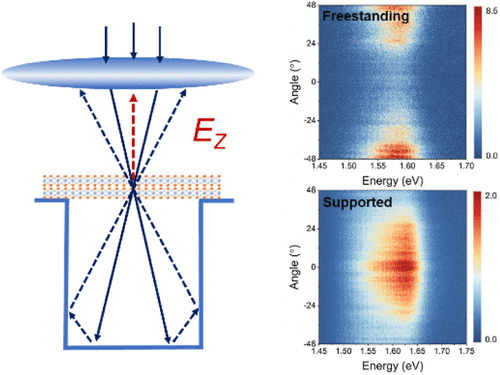
![BryanKeIIy's tweet photo. [PDF] Very strong light-matter coupling in patterned GaAs heterostructures🛸](https://pbs.twimg.com/media/HKJD6mkWMAAac5U.jpg)