Want to make the slimmest USB C PCB ever? These footprints are now open source, and in public domain!
Enjoy! Make sure your PCB is 0.6 mm thick, and show me the cool stuff you make with them.
https://t.co/PHcypdLK5f
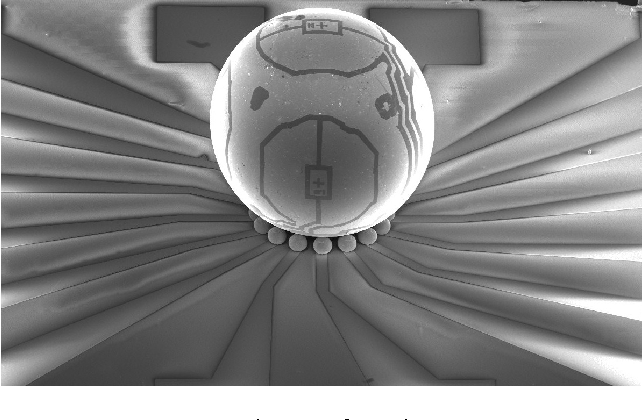
At the peak of the dot-com era, Ball Semiconductor was a crazy silicon fab.
Founded by ex-Texas Instruments folks, the idea was (you guessed it) to etch using spherical photolithography.
They had some success with the process! But the company failed dramatically.
Just found out about these right angle SMD component adaptors...
I mean you REALLY need to mount a magnetic sensor at right angles...
kinda based ngl....
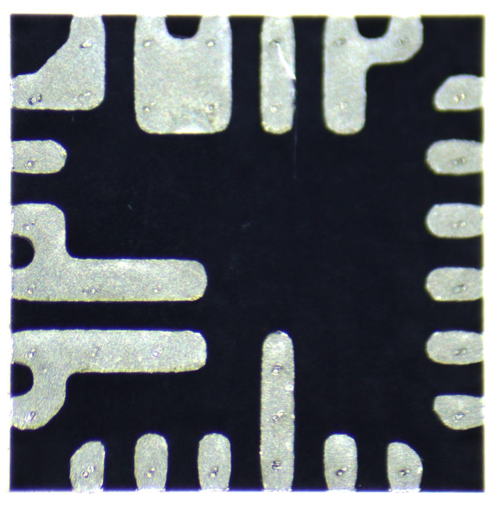
@redshirtjeff@RshnThms@cursedconnector It's a fiducial mark, usually you have between 1 and 3. They are used to precisely calibrate the placement of the PCB for pick and place machines
@redshirtjeff@RshnThms@cursedconnector It's a fiducial mark, usually you have between 1 and 3. They are used to precisely calibrate the placement of the PCB for pick and place machines
@cursedconnector@qlavash@Einthecorgi2 Tweetdeck is dead so it's a bit annoying, but I have enouhg PTSD from each footprint that I've shared: https://t.co/HU9yCkjkcx