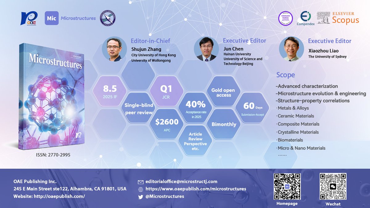
Why follow @Micro_OAE? 🔬
JCR Q1 | IF: 8.5 | Open-access, peer-reviewed journal.
Follow for:
• New papers & commentaries
• Special issue opportunities
• Hot topics in advanced materials
Tag your research team & co-authors!
#Microstructures#MaterialsScience
@BryanKeIIy Good articulation of the coupled environment. Curious what dominates first in practice: dielectric performance drifting with temperature, or the absorber's microstructure and oxidation stability breaking down? That usually decides the whole design strategy.
@kaistpr 94% retention after 100 cycles at 4C is a genuinely strong number—dendrite suppression is where most fast-charging claims quietly fall apart. Curious whether the liquid-crystalline ordering holds up under high areal capacity and in larger cells. Nice work, KAIST.
@SeoulNatlUni Reducing scattering while keeping the pore network open is the hard part—usually you trade one for the other. Impressive that both survive. Curious how far this scales to thicker parts or higher filler loading. Nice work, Prof. Shin's team.
@mit_dmse@UTAustin Wonderful topic. Nitrides keep reminding us how much strain and defect engineering matter for real function—precisely the processing–property connections we care about at Microstructures. Looks like it was a great session! @UTAustin
@TBrezesinski@NatureComms@BIT1940@PKU1898 Great collaborative work! Fast‑charging all‑solid‑state Li‑S batteries are highly promising. What microstructure‑related bottleneck do you think is the biggest barrier for practical deployment? Congrats to the team! #BatteryResearch
@NanotechnoWorld This aligns well with our focus on microstructure-driven functional property design. Atomic-level understanding is key to translating lab discoveries into manufacturable devices.
Great work on hafnia ferroelectricity! Tuning atomic structures of existing oxide layers is such a promising route for next-gen silicon-compatible memory & capacitors. What’s your take on the biggest remaining challenge?
#Microstructures#Hafnia#Ferroelectrics#Semiconductors
Harnessing atomic structure to advance semiconductor technology
Researchers led by Rohan Mishra at Washington University in St. Louis have uncovered why hafnia, the insulating layer in silicon transistors, becomes ferroelectric when grown extremely thin. Rather than forcing it into a conventional ferroelectric phase, they found that stabilizing an antiferroelectric structure and switching it electrically offers a more practical route to memory storage and high energy density capacitors.
The team combined quantum mechanical modeling with atomic resolution electron microscopy and single crystal film synthesis by collaborators at the University of Nebraska-Lincoln and Georgia Tech. In a related study on zirconia, they observed ferroelectric domains smaller than one square nanometer and predicted that the domain walls could conduct electricity and respond to an electric bias, hinting at atomically thin memory components.
Because these oxides are compatible with existing silicon chip manufacturing, the findings suggest engineers can tune electronic behavior at the atomic level without introducing new materials or components. For researchers, the work also shows how tightly pairing theory with microscopy can resolve long standing puzzles in thin film behavior.
https://t.co/Ttj4EiFovF
AM-built metals vs bulk metals — why do the mechanical properties differ?
Prof. Jan Van Humbeeck (KU Leuven, Additive Manufacturing)
11 Nov · 09:00 UTC / 17:00 Beijing.
Free registration: https://t.co/xwREWfyPvS
#AdditiveManufacturing
📢Webinar Alert
Why do AM‑fabricated metals show different mechanical properties vs bulk materials?
🎤Prof. Jan Van Humbeeck (KU Leuven)
11 Nov 2026 09:00 UTC | 10:00 Brussels (UTC+1) | 17:00 Beijing (UTC+8)
Register: https://t.co/xwREWfyPvS
#AdditiveManufacturing
Which bottleneck slows down AI-driven microstructure prediction? #AI#Microstructures
Is it limited experimental data, poor out-of-distribution generalization, insufficient physical constraints, or interpretability? We’d love your opinion.
🔬 OAE is at the 10th International Forum on Materials Genome Engineering! @HaoLiLab_DigCat@materialsgenome@ENGEnergy_@maxplanckpress@unibirmingham@UniofOxford@NIMS_PR@Octopusrok@USTB1952
We are excited to join the forum in Jinan, Shandong (Nov 2–6, 2026), bringing together leading researchers in AI-driven materials design, high-throughput experimentation, materials big data, and “AI + New Materials” applications.
📍 Visit us at Booth B-3 to connect with our editorial teams and explore submission, collaboration, and publishing opportunities.
Our journals on site include: ⚡ Energy Materials @OAE_EnergyMater 🔬 Microstructures @Micro_OAE 🧪 Chemical Synthesis @Chem_Synth 🌱 Soft Science @OAE_SoftScience 🤖 Journal of Materials Informatics @OAE_JMaterInf 🧠 AI Agent @ai_aiagent 🌀 ZEntropy 🧩 Metamaterials Science 🔩 Micro Nano Science 🔋 Energy Z
Whether you work on computational materials design, intelligent experiments, materials data infrastructure, or industrial applications in energy, chips, advanced equipment, and biomedical materials, our team would be glad to meet you in Jinan.
👋 See you at Booth B-3!
MaterialsGenomeEngineering
#MGE2026 #AIMaterials #MaterialsInformatics #OpenAccess #OAEPublishing #EnergyMaterials #JMI #AI4Materials #Jinan
Can selective oxidation create buried ferromagnetic nanolayers in #NiMn alloys? New work reveals MnO/Ni‑rich/NiMn trilayer structure with ferromagnetic Ni‑rich subsurface.
By Michael Farle and Zian Li et al.
👉https://t.co/jyqPwwyoLi
#Magnetism#Oxidation#Microstructures
📑Can oxygen octahedral engineering tune magnetic anisotropy in #SrRuO₃?
Thickness‑driven symmetry transition between tetragonal and orthorhombic phases tunes magnetic behaviour in epitaxial films.
👉https://t.co/kVJ4Yfvx1o
#OxideThinFilms#Magnetism#Microstructures
Another media outlet is highlighting our work on a simple and scalable approach to converting residual heat into electricity using thermoelectric materials (DOI: 10.1016/j.mtener.2026.102363). Thanks @cbm_noticias!
Read the full story 👇
https://t.co/FRKfn6htzz