@dnystedt@Mikeair899 Please tell us how the reporter knows. Who in hell at TSMC or Nvidia will leak such information, 2 weeks after GTC and Rubin Ultra roadmap + servers introduced.,,
Typical Samsung out of touch propaganda. Number on PowerPoint. Single digit real world yields, even years after introducing a new tech. Cough GAA cough
Samsung to Adopt 'Fork Sheet' for 1nm Process… All-Out Effort to Win Over Big Tech
Samsung Electronics' foundry division has set a target to introduce 1nm (nanometer; 1nm = one-billionth of a meter) process technology by 2031. The 1nm node is dubbed a "dream semiconductor" process, in which computing elements the width of just five atoms are arranged using an entirely new method. The goal is to engage in a head-to-head technology race with rival TSMC and seize leadership in the next-generation semiconductor market. Samsung is also developing a variety of process variants at its current cutting-edge 2nm node to secure major customers.
Fork Sheet Adoption… Aiming for a Fine-Pitch Process Breakthrough
According to industry sources on March 30, Samsung's foundry division plans to complete R&D on a 1nm semiconductor process by 2030 and transfer it to mass-production lines. The 1nm node is regarded as a dream-level innovation: it implies that the width of transistors—the elements responsible for data processing inside a chip—can shrink to just 1nm. Because that is half the transistor width of Samsung's current cutting-edge 2nm technology, process complexity rises significantly.
Alongside transistor scaling, the 1nm node will also introduce a new architecture called the "fork sheet." Up through the 2nm node, transistors have been built using Gate-All-Around (GAA) technology, which maximizes power efficiency by wrapping the gate around the channel on all four sides instead of three. The fork sheet takes this further by minimizing the spacing between GAA transistors. The technique inserts a non-conducting wall between GAA devices—much like driving a fork between them. Think of it this way: in a conventional layout, houses in a village are separated by open lawns; with fork sheet, those lawns are replaced by massive concrete walls. Just as removing the lawns frees up space to build more houses, fork sheet allows more transistors to be packed into the same chip area.
Chasing No. 1 TSMC
Samsung's foundry division ranks second globally, trailing TSMC—which commands nearly 70% market share—by roughly a factor of ten. TSMC, despite its dominant position, is also known to be pursuing fork-sheet adoption for its own 1nm-class process beyond 2030. Industry observers see Samsung's decision to lay out a 1nm roadmap targeting 2030 as a signal that it is preparing to compete with TSMC on equal technological footing.
Since announcing its "No. 1 in System Semiconductors by 2030" vision in 2019, Samsung has maintained a strategy of matching TSMC on leading-edge nodes. It was the first in the world to introduce extreme ultraviolet (EUV) lithography at the 7nm node in 2019, and the first to adopt GAA transistors at the 3nm node in 2022. An industry official noted: "It is realistically difficult for Samsung to overtake TSMC in revenue or production scale, but it continues to compete on the technology front. A prime example is last year's $16.5 billion (approximately KRW 25 trillion) contract with Tesla to supply 2nm AI chips—a milestone built on technological capability."
Rapid Diversification at the 2nm Node as Well
Samsung's foundry division is also rolling out multiple enhanced variants of its current cutting-edge 2nm technology. It is developing a custom process called "SF2T" for mass production of Tesla's 2nm AI chip, "AI6." Production of this chip will begin in 2027 at Samsung's new foundry hub in Taylor, Texas.
The division is also accelerating development of "SF2P," a new 2nm process to be deployed starting this year for manufacturing the next-generation smartphone application processor (AP) from Samsung's System LSI business, as well as "SF2P+," slated for activation next year. A semiconductor industry source said: "With 2nm process yields now exceeding 60% at peak, productivity has improved, and expectations for a return to profitability this year are growing."
@RehanYawar84469 On what chip? a tiny DRAM die? a simple design like these Chinese mining ASICs with large SRAM arrays, regular structures and few mixed signal/analog blocks? Truth is that nobody trust Samsung marketing. Take everything they say with a truckload of salt
@HyperTechInvest When I saw the Korean articles ditching Micron, I immediately call the BS. Same story happened with H200. No idea why people is always wrong with Micron
🚨 NVIDIA JUST ANNOUNCED DATA CENTERS IN SPACE
Jensen Huang:
>we’re going into space
>we’ve already been out in space
>announces “Vera Rubin Space-1”
>"in space there's no conduction, no convection, just radiation"
>"we have to figure out how to cool these systems in space"
>"we've got lots of great engineers working on it"
GPUs IN SPACE INCOMING
JENSEN TO MICRON CEO: To my friends at Micron. Our partnership changed the world. Industry’s fastest HBM4 delivered to NVIDIA.
Seems like Micron HBM4 is a go.
$MU $NVDA @MicronTech@NVIDIAGTC
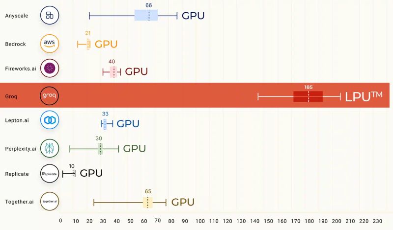
@canyoudugit8@TickerSymbolYOU you clearly don't understand the market. LPU is for small models that require ultra low-latency. No rack to rack here. In fact, no inference requires rack to rack. Scale-out is for training.
Have a nice day dreaming of 5% market share AMD taking over Nvidia with MI455X NPU lol
@canyoudugit8@TickerSymbolYOU if you cant understand that AMD NPU is a simple old school bunch of VLIW tiles that no bandwidth can compensate for it's inefficiency vs LPU novel software deterministic tensor-streaming engine optimized for inference, then let's agree to disagree and time will tell
LOL no, that's not how it works.
1/ KV cache transfer isn't the bottleneck in Rubin + LP30. BlueField-4 STX boost throughput by 5x. Actual inter-LPU bandwidth is 2.5 TB/s bi-di per chip.
2/ AMD 15 TB/s internal? yeah nice for integrated decode, but LPU deterministic arch (static scheduling, not Von Neumann waste) wins in overall latency & speed.
3/ Benchmarks already show LPUs crush NPUs and with much less bandwidth than the Rubin solution.
Groq journey at Nvidia:
LP30 is a quick last minute addition.
LP35 blends into Nvidia software ecosystem (NVFP4).
LP40 adds Nvidia interconnect (NVLink).
LP-Next will co-packaged on-die.
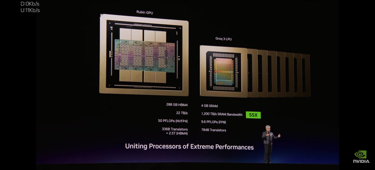
OK here we go. Same architecture, scaled up. 500 MB SRAM per chip. Jensen saying up to 25% of your datacenter could be groq. 8 way systems for 4 GB SRAM. Use dynamo for attention Decode only. Working over ethernet on special mode to half latency. Samsung LP4X. Ship in 2H/3Q.
@canyoudugit8@TickerSymbolYOU 1/ LPU is different than NPU. Apples vs oranges
2/ LPU is much faster (low latency software deterministic execution with static scheduling vs classic Von Neumann arch that is less efficient for inference)
3/ AMD NPU lacks Nvidia ecosystem, it will go nowhere
@paurooteri In VR300 (Vera Rubin Ultra) we have 2x 1TB GPU HBM + 2TB CPU LPDDR5X (=4TB total) as coherent memory pool for KV Cache (thanks to NVLink-C2C) per compute blade. That's an increase of 4.6 times memory capacity in a single generation (vs GB200).
N3 capacity was set when Nvidia wasn't targeting top nodes & was smaller TSMC client than Apple.
It changes with Feynman: Nvidia is lead customer for A16 node, booking all early capacity like Apple once did.
Called it
@dylan522p just dropped the numbers: NVIDIA owns 70% of TSMC N3.
Google Cloud and DeepMind can’t agree on how many TPUs to give Anthropic.
Hard to be generous with chips you can’t guarantee for yourself.
One CEO controls delivery. That’s where the power sits. $nvda
Honestly, I thought this paper was written by captain obvious. No disrespect but memory bandwidth/capacity were always the bottleneck. But we live in real world, not lalaland, so things like manufacturing capacity and supply chain restrictions made the ASICs/TPU/GPUs what they are today. Unless you believe that all these silicon engineers are stupid...
Corrections:
1. Old news. it was done 2 months ago.
2. Timing adjustments are done until very late in the qualification process. Each cycle is the same and each cycle same outlets publish FUD. Boring.
3. BS. Samsung will love to take more market share with Nvidia.
4. Taken by others (Foxcom and Quanta).
5. no comment. I don't follow DDR4.
@jukan05 "Groq, AI Chip Startup Acquired by NVIDIA, to Ramp Up Production at Samsung Foundry"
When the title is already wrong, how can you trust this article?