Why would NVIDIA put part of a GPU inside a memory stack?
Seoul Economic Daily reports that NVIDIA wants the bottom die of its custom HBM, called NVHBM, built on TSMC's 3nm logic process. That is an advanced logic process for part of a memory stack. NVIDIA's design helps explain why: the base die takes on a job the GPU used to do.
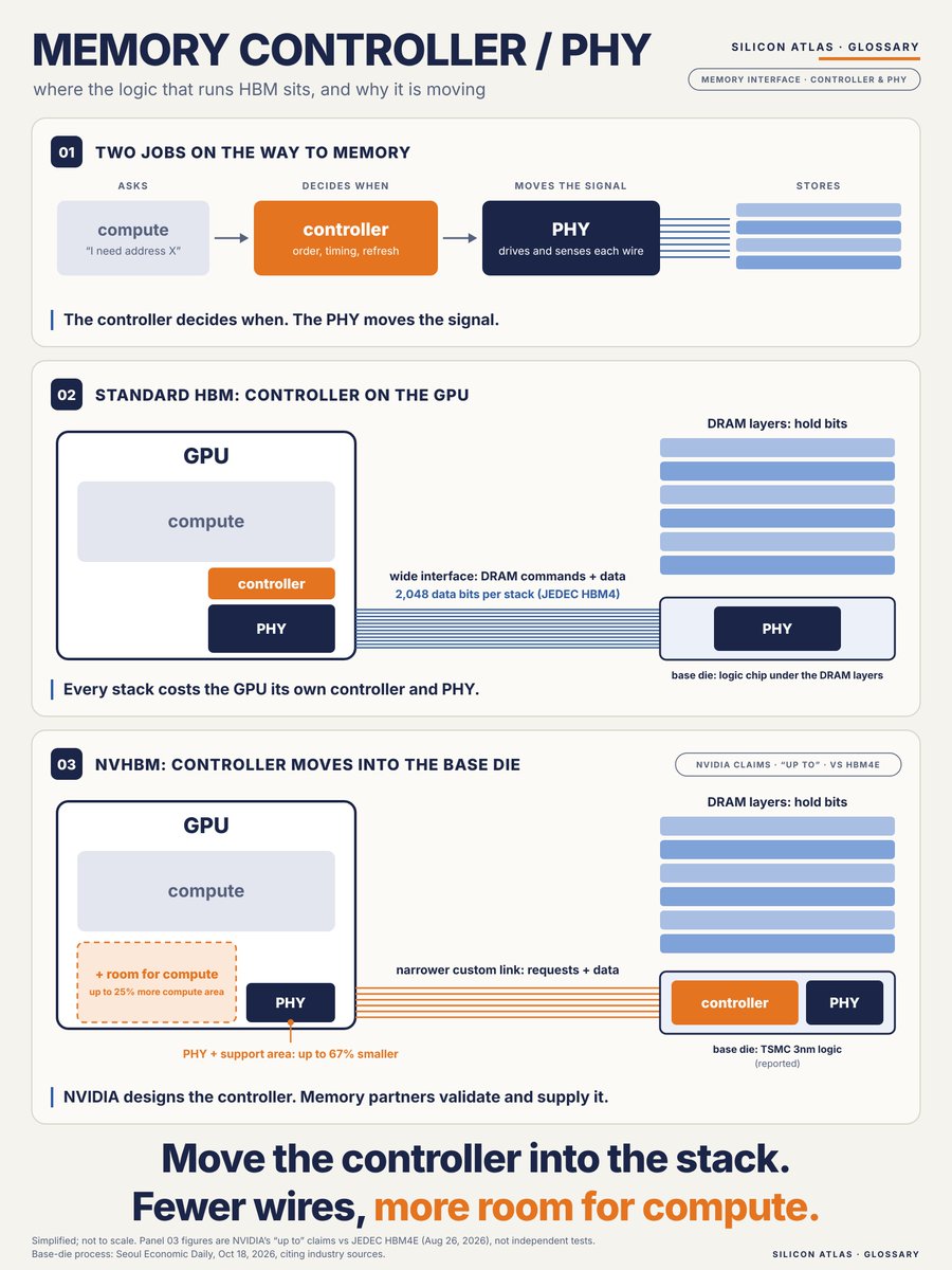
Two jobs sit between a GPU and its memory. A PHY drives and senses the signal on each wire. A memory controller decides when to read, write and refresh.
A memory controller is the logic that turns "I need this data" into DRAM commands, sent in the right order and at the right time.
In standard HBM, the GPU holds the memory controller and its own PHY for every stack. NVHBM moves the controller into the base die, under the DRAM layers, and pairs it with a redesigned PHY. Together, these allow a narrower custom link and leave more of the GPU for compute.
Think of a head office that used to schedule every shelf pick in its warehouse. Now it sends orders, and the warehouse runs its own floor.
NVIDIA says NVHBM gives up to 30% more bandwidth per stack and 15% lower HBM power than standard HBM4E. These are vendor figures, not independent tests. Amazon's Annapurna Labs is the first named partner, but no first chip has been named.
NVIDIA designs the controller. Memory partners validate and supply it.
The memory still holds the bits. The logic that decides when they move now sits right under them.
@Wbackdown It’s real. The vLLM team reported about 2× faster token generation with EAGLE 3.1 on Kimi K2.6, using four GB200 GPUs for a single-user coding workload. The key is accepting enough draft tokens to make the extra work worthwhile.
A slow local AI assistant doesn't automatically need a new GPU.
When an assistant quotes a document, much of its next text is predictable. Speculative decoding drafts several pieces ahead and checks them together, reducing sequential model passes when those guesses are accepted.
If the workload already fits in memory, I'd test this before replacing a $NVDA GPU, comparing complete tasks at the same quality. I expect better inference software to extend older GPUs' useful lives.
@Wbackdown@SemiAnalysis_ Yes, it shows up in latency. AMD’s DeepSeek-V4.1 test on two MI355X GPUs cut layer time from 209 to 122 μs at concurrency 1. That’s the fused path, including communication, rather than just a cleaner compiler graph.
Four days ago @SemiAnalysis_ said AMD got megakernel decode into vLLM first. This is NVIDIA's answer, and it shows "megakernel" names a direction, not a single number.
Research versions run a whole decode step as one GPU program. AMD's new vLLM path uses two launches per layer. NVIDIA's Kimi K3 path cuts each layer from 23 kernels to 13, per the vLLM write-up: closer to heavy kernel fusion than one long program.
All three go after the same waste: the idle time between short GPU programs. The next one has to start, every worker waits for the slowest, and weights aren't loading yet.
That idle time matters most when few users are on the chip. NVIDIA's numbers on GB300 (16 GPUs, no speculation): 1.88x at batch 1, 1.62x at batch 64.
The gain holds up better at batch 64 than AMD's did. The NVIDIA work also merges the cross-GPU sum into compute and prefetches weights, so not all of it comes from removing gaps.
Fewer launches, fewer gaps. How few counts as "mega" is still being argued.
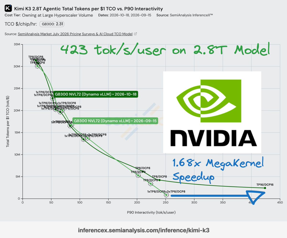
BREAKING NEWS🚨: NVIDIA has just achieved 423 tok/s/user 🚀 on the 2.8T Parameter Kimi K3 model via a new upstream vLLM optimization. 1.68x Faster on the Same Hardware!
This was done by NVIDIA CentML's Benjamin, who wrote NVIDIA's new decode-specialized kernels in Cute DSL via aggressive Megakernel fusion. This is a 12,000 LoC Megakernel and is the future of advanced AI-assisted kernel generation. NVIDIA is already working on DeepSeekv4.1 and other models for vLLM too.
Someone should give this NVIDIA 10x engineer a raise for this great new major feature!
HBM rivals are chasing a moving target.
In an October 2 report, $SKHY said it tested FemtoMetrix’s non-destructive inspection in DRAM and HBM processes, then decided to deploy multiple tools per fab.
Buying the tool is one step. Knowing which signals reveal a process problem, and how to fix it, is where accumulated production experience matters.
I expect experienced HBM suppliers to turn better inspection into yield improvements faster, raising the bar for DRAM challengers like CXMT.
That reinforces my preference for HBM. The full article connects manufacturing barriers to demand, supply ramps and the contracts that could sustain earnings:
https://t.co/H1C6ocU0uc
@PhotonCap I also prefer those names but Neoclouds matter to the whole AI ecosystem, including the hardware suppliers. I’m hoping for them to secure the financing they need to keep building.
@RonfortMartin Yes, I quoted that report too. Nvidia is really pushing for a common base-die process as part of NVHBM. For Samsung, winning that HBM business can matter more than keeping every step in-house.
SK hynix is a top HBM maker. So why does TSMC build the bottom die of its HBM4?
SK hynix stacks its HBM4 memory on a base die made on TSMC's 12nm-class logic process. Samsung makes its base die in its own logic foundry. The memory comes from a DRAM line. The logic under it does not.
That split comes from what each process is built for.
A logic transistor is built to switch fast. It balances speed, power and leakage.
A DRAM cell transistor switches on to read and write, then must barely leak, so a tiny charge lasts until refresh. So DRAM makers bury its gate in the silicon. The path bends under the gate, and the longer path leaks less.
The capacitor is the other big difference. DRAM builds rows of tall capacitors, and those memory steps run hot for hours. The sense amps and drivers are built first, so they must survive that heat. That limits which logic transistors can share the wafer.
HBM has always had a base die under the memory stack. It handles the link to the GPU. Through HBM3E, SK hynix built it in house. For HBM4 it moved that die to TSMC's logic process to fit more functions into limited space.
Samsung's bonded 4F² prototype takes a different route. It puts the cell array and its periphery on separate wafers, so each can be optimized on its own.
Watch who makes HBM4E base dies, and whether the first 4F² DRAM ships with its logic on a second wafer.
Same silicon. Different jobs.
@Gray99999999 I like the piggy bank and abacus analogy. Keeping charge and switching fast are very different jobs. That’s exactly why the process choices differ.
Why would $Samsung use $TSM when it owns a foundry?
Seoul Economic Daily reports $NVDA wants all three HBM suppliers to use TSMC's 3nm process for the logic beneath its custom memory stacks, reducing supplier-specific design and validation work.
My take: the customer's design requirements can outweigh Samsung's advantage of making both memory and logic in-house. Winning the HBM order can mean sharing manufacturing revenue with TSMC.
According to Korean media reports, Samsung Electronics has decided to manufacture the NVHBM base die using TSMC’s 3nm process at Nvidia’s request. However, Samsung has not entirely ruled out using its own foundry and is also validating whether it can produce the base die in-house in case NVHBM demand exceeds TSMC’s production capacity.
https://t.co/3WNR660C24
@WDChokepoint Good question. Module specs alone wouldn’t tell us. An independent teardown showing the cell layout and cross-section would be the clearest way to check.
4F² DRAM promises smaller cells. Why doesn't that mean more supply overnight?
On Oct 10, CXMT said it targets a year-end launch for its first 4F² DRAM, a server DDR5 module. Three days later, Samsung and SK hynix each fell more than 7% in Seoul. Some analysts called it profit-taking.
4F² is the cell's footprint: four times F squared, where F is the process's smallest feature size. Today's DRAM cells take six.
The gain comes from the cell layout, even at the same feature size. The transistor's channel stands up instead of bending under the gate. CXMT says it wraps the gate around that upright channel to cut leakage.
Today, the cells and the support logic sit side by side on one wafer. Samsung's 2026 prototype split them: cells on one wafer, bonded on top of a logic wafer. CXMT has not said whether its first product does this.
If it does, there is a catch. Wafer-to-wafer bonding can't pick good dies to pair, so a bad die can leave its good partner unusable. Either way, the new transistor is hard on its own. New flows usually start at low yield.
Density at the same feature size is especially valuable to a company that cannot buy EUV scanners.
CXMT gave no capacity, speed or volume. Korean reports say the first parts may use 4F² only in part. Watch for chip specs, customer qualification and steady volume shipments.
The cell got smaller. The factory got harder.
@GiovanniZibordi Thanks for sharing this with your Italian readers, Giovanni! Strong AI demand and the cost of funding it are both worth understanding.
@skewpilot This isn’t fearmongering. I wrote this to explain the financing concerns people are discussing. Anyone who follows my posts knows I’m highly bullish on the AI cycle. That doesn’t mean every company’s financing works out. Disagree with the argument, but keep it respectful.
Why does a company with $104 billion in contracts still lose money?
CoreWeave sells GPU computing for AI. In Q2 2026 it brought in $2.58 billion in revenue and reported about $104 billion in backlog. It still posted a $626 million net loss.
Its net interest expense that quarter was $640 million.
Before interest, the business was close to breakeven, with an operating loss of $49 million. Interest turned a small loss into a large one.
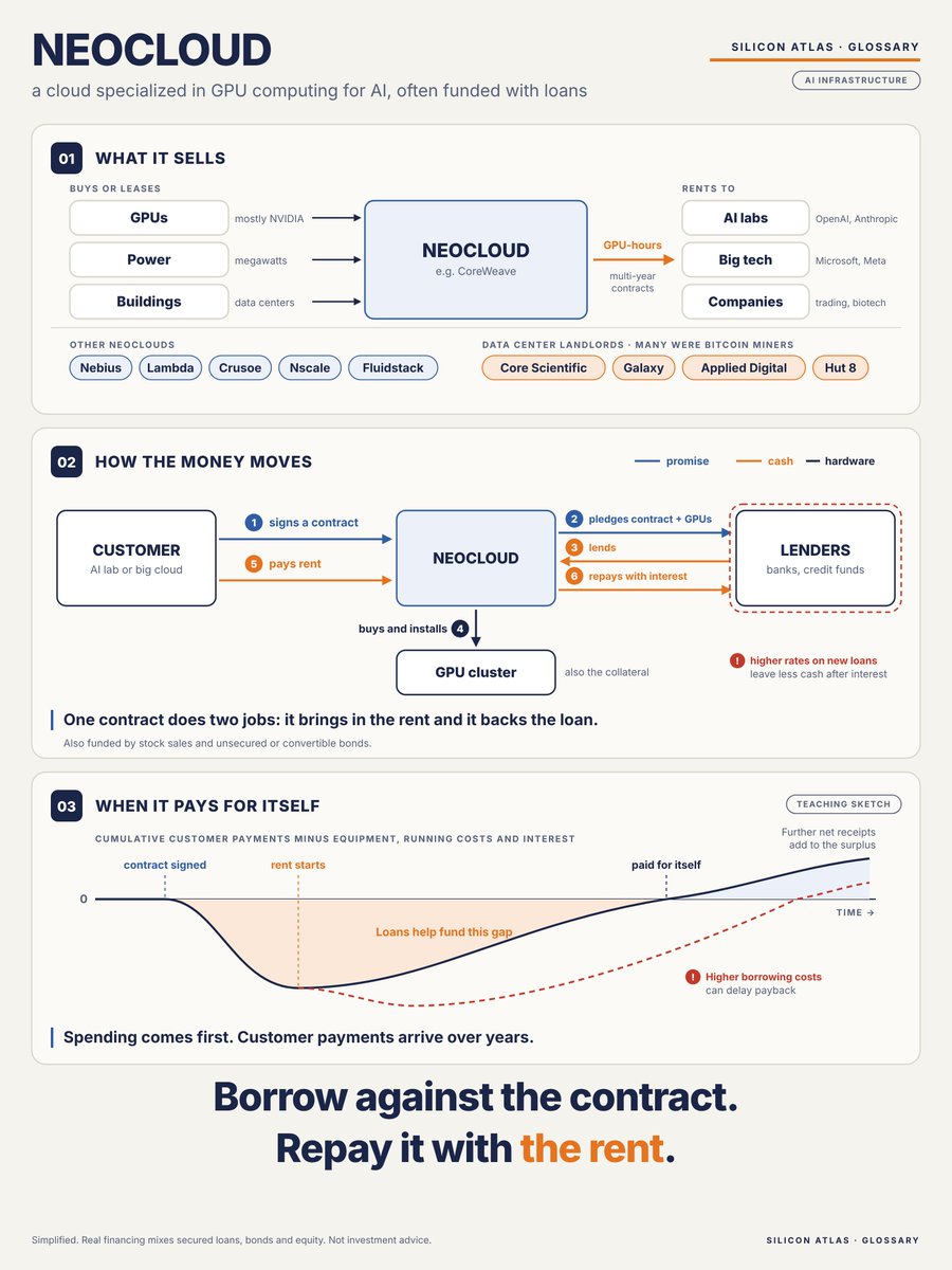
Why so much debt? GPUs are paid for before a cluster goes live, while customers pay over several years. On the income statement, that equipment cost is spread out as depreciation. Much of the cash spending comes before the customer payments. Loans help bridge that gap. CoreWeave borrows against signed customer contracts and the GPUs themselves, so one contract brings in revenue and backs the loan.
A neocloud is a cloud company specialized in GPU computing for AI. Nebius, Lambda, Crusoe and Nscale are others, each funded differently.
Think of a landlord who signs the tenant, borrows to build, then repays the bank with the rent.
That is why financing conditions matter. This week, some CoreWeave bonds traded at yields around 15%, signaling pressure on future borrowing costs. Existing fixed-rate interest payments do not automatically rise.
A large backlog helps secure financing. It does not guarantee a profitable buildout. The real test is whether customer payments recover the equipment investment and financing costs, while arriving in time to meet debt payments. Not investment advice.
@Autonn254315@lothran1 That would be a much bigger problem. The debt would still need paying while customer cash disappeared. I’d separate that risk from the funding gap today: which contracts can be cancelled, and whether customers can keep paying.