$ensi/ $ensif up 22% today in GB.
The Bottom Line: EnSilica doesn't need a miracle; it just needs to execute on the $400M+ pipeline it already has. If they convert even 30% of those leads into long-term supply contracts, the math for a multi-billion dollar valuation becomes real
It's legit coincidence that it's catalyst ( $JBL ) after catalyst (Nasdaq listing) after catalyst ( $GOOGL + $MRVL ), after catalyst ( $GFS ), after catalyst ( $GFS + $AMD ).
Alongside $NVDA investing into CPO everywhere.
I just timed my long after OFC but did not expect all of this lol.
@aleabitoreddit@FractalVeritas It's also not as restricted to scale out laser manufacturing. Theres technical challenges with the manufacturing but no regulatory hurdles
In order to really understand the $LPK/ $LPKFF thesis, you need to be able to answer two simple questions:
1. Why Glass?
2. Why Now?
If you can’t, don’t worry. I’ll do the heavy lifting for you:
1. Why Glass?
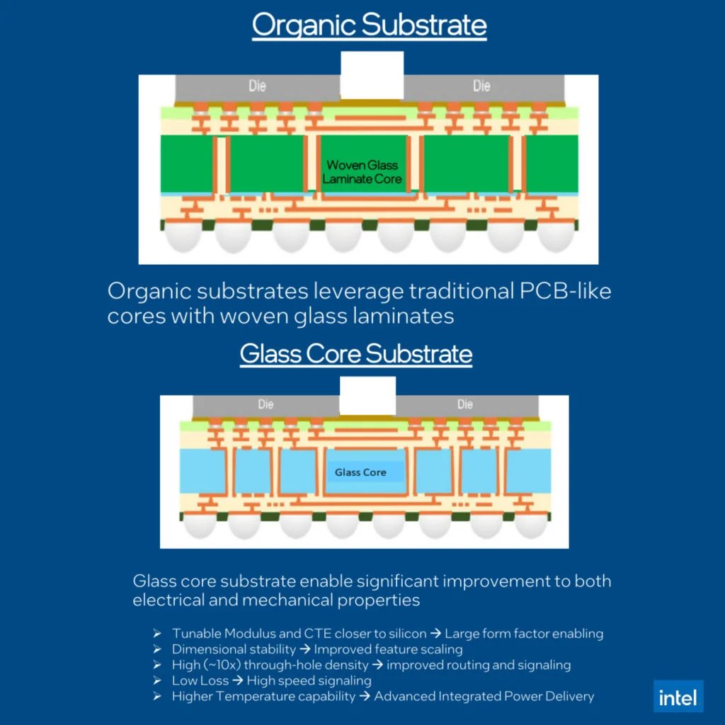
Every chip you've ever used sits on top of a substrate. Think of it as the foundation of a building--it redistributes electrical signals between the chip and the motherboard. For the last 20 years, that foundation has been made of organic materials. ABF (Ajinomoto Build-up Film) became the industry standard. It's cheap, it works, and it scaled well enough to get us to where we are today
But organic has problems. The internal structure is non-uniform--messy at the atomic level. It warps under heat. It bends under mechanical stress. The wiring resolution is limited because you can't do precise lithography on a surface that isn't flat. And as chips get bigger and hotter, these problems compound. There's a reason $NVDA's Blackwell had thermal issues--we're running into the physical ceiling of what plastic can handle
Glass is the step change which solves all our problems at once:
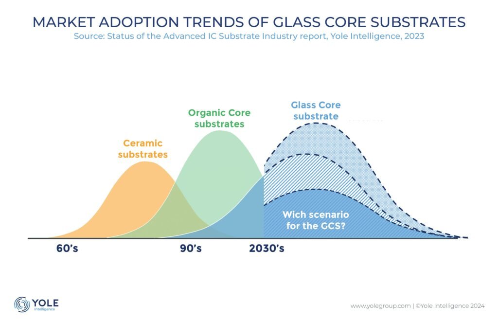
It's rigid. You can build substrates over 100x100mm without distortion (larger substrates = better margins). Georgia Tech demonstrated 60 chiplets on a single glass substrate--roughly 4x what's possible on $TSM's current CoWoS. More chiplets, more transistors, more compute per package
It's atomically flat and smooth. This means finer lithography, tighter component spacing, fewer defects, better yields. The kind of precision that organic materials structurally cannot deliver
It has a low dielectric constant. Less parasitic capacitance, faster signal propagation, higher frequencies. The substrate stops being a bottleneck for chip speed
It's thermally stable up to 600°C with a CTE (coefficient of thermal expansion) up to 5x lower than organic and nearly identical to silicon. Both contain silicon atoms--they expand at (pretty much) the same rate under heat. No warping, no cracking, no connection failures. Even on the largest designs
Rectangular panels (650x650mm) instead of round wafers. More chips per panel, less waste. Better unit economics at scale
Glass is the step-function to organic which the industry is so desperate for!
Why Now?
Because AI broke the old roadmap. Simple as that!
The demand for AI acceleration and high-performance computing has pushed chip design into 2.5D and 3D packaging--stacking multiple dies vertically, integrating CPUs, GPUs, HBM memory, all in a single package. The packages are getting physically larger and thermally denser at a pace nobody expected five years ago
Organic substrates were supposed to carry us through the rest of the decade. They won't. The industry is already running into thermal and dimensional limits on current-gen AI chips, and next-gen designs (think 1 trillion transistors per package by 2030) will be impossible on plastic. The breaking point isn't theoretical--it's happening now
That's why every major player is moving simultaneously:
- $INTC: $1B+ invested, dedicated glass facility in Chandler AZ, fully functional glass-core prototype, targeting mass production 2026-2027
- $TSM: developing glass for Fan-Out Panel Level Packaging, driven by NVIDIA demand
- Samsung Electro-Mechanics: already sampling glass substrates to Apple and Broadcom, targeting 2027 mass production
- Absolics (SKC): $600M dedicated glass fab in Georgia, first CHIPS Act recipient for glass
- LG Innotek: pilot line underway, targeting 2028
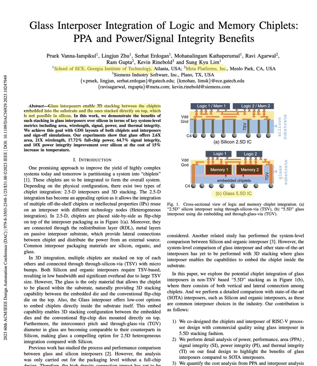
- Meta + Georgia Tech: published 5.5D packaging research on glass showing major improvements in area, power, and signal integrity
This isn't R&D curiosity anymore. This is capex being deployed, pilot lines being built, and customer qualifications underway. The industry has collectively decided that glass is the next 20 years of semiconductor packaging.
I'm positioning accordingly
This is really cool! $SIVE
@ParadisLabs Shared with me this morning that Sivers shared my deep dive report on their LinkedIn account
So cool to see the recognition!
If you want to read it yourself, check it out here:
https://t.co/RVE4xnUbyQ