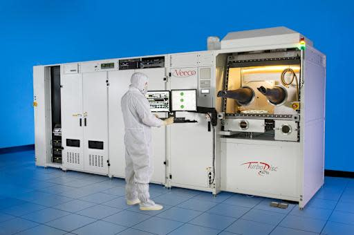
Aixtron $AIXA announced today that Lumentum has ordered multiple G10-AsP MOCVD systems for InP-based laser and detector production, driven by surging demand from AI datacenter networks. The InP epitaxy buildout is accelerating.
Together with the constraints on InP substrates, this is currently, in my view, the biggest bottleneck for InP Lasers.
Every one of these new reactors ships with LayTec in-situ metrology. That part is well known. Less appreciated is that LayTec is expanding revenue beyond sensor modules with a second, very different product.
In a recent update, LayTec is quietly scaling its EpiX C2C mapping station as a second revenue pillar.
Most investors associate LayTec with sensor add-ons on MOCVD reactors, like those in every Aixtron G10-AsP ordered by Lumentum. The EpiX C2C is fundamentally different: a standalone, fully automated production tool with cassette-to-cassette wafer handling, FOUP load ports and wafer-ID reader. This is fab-floor equipment, not an accessory.
EpiX scans finished epitaxial wafers point by point and builds a full 2D map showing whether layer thickness, composition, and light emission are uniform across the wafer, essentially a quality control step before the wafer moves into the next process stage.
LayTec has also introduced pre-configured product packages for two fast-growing compound semiconductor markets:
InP Optoelectronics, optimized for NIR photoluminescence mapping of InP laser and detector structures (900–1700 nm), used in AI datacenter transceivers and CPO GaN Power Electronics,or AlGaN barrier composition and thickness mapping in GaN-on-Si wafers, relevant for EV infrastructure and datacenter power delivery.
Previously, EpiX required custom configuration per material system. Now standardized application packages with pre-programmed analytics reduce adoption friction and shorten sales cycles as demand rises.
With EpiX C2C, LayTec monetizes each fab beyond in-situ sensors. A typical workflow now spans three touchpoints: in-situ epitaxy monitoring, ex-situ wafer mapping via EpiX, and in-situ plasma etch monitoring. Revenue per fab becomes multiple times higher than a single sensor add-on.
LayTec appears to be very well positioned and strategically prepared for the accelerating demand in InP and GaN applications. If LayTec were a standalone company, this would look like a classic picks-and-shovels compounder. As part of Nynomic’s photonics portfolio, it sits in a group trading at ~1.2x sales, with LayTec likely contributing ~15% of revenue.
In my view, the potential for LayTec is still underestimated.
Agree that $MRAM is a growth/monopoly and PE this high demonstrates this. It is drawing a lot of attention and since it's designed for space/defense would be nice if it can secure some of private/public space/defense contracts with companies like SpaceX to support future valuations as long as execution is not an issues.
From grok
"Everspin is the sole volume manufacturer of Toggle MRAM. https://t.co/bVsShKltEq
This gives it a clear monopoly on the specific Toggle cell design (patented, field-switched architecture optimized for high reliability, unlimited endurance, and extreme environments). No other company produces Toggle MRAM at commercial scale.
Broader MRAM competitors exist, primarily in spin-transfer torque (STT-MRAM), a different switching technology that is more scalable for higher densities but trades off some of Toggle’s extreme reliability advantages:
• Avalanche Technology: The main direct competitor in high-reliability/aerospace/defense MRAM. They offer STT-MRAM products positioned as drop-in replacements for some Everspin Toggle parts in industrial applications and target similar rad-hard markets. (They have also pursued patent disputes with Everspin on STT-related IP, but Toggle remains Everspin-only.)
• Others (research or limited): NVE Corporation (smaller niche MRAM), plus historical R&D from Samsung, Toshiba, etc. No one else has commercialized Toggle.
In non-MRAM persistent memory, substitutes like FRAM/FeRAM exist, but Everspin actively positions Toggle MRAM as a superior replacement (unlimited endurance vs. wear-out issues in FRAM). Overall, the Toggle-specific monopoly is a key differentiator for defense, industrial, and automotive uses requiring the highest robustness. https://t.co/P0iG5h0stq
There is no consensus “expected price increase” specifically tied to the monopoly—analyst targets remain conservative despite the positioning. https://t.co/stiddHuWSl
As of May 2026 (post the stock’s recent surge to the mid-$20s amid the $40M defense contract news), the 1–2 analyst consensus 12-month price target is around $18–$18.50 (e.g., Needham’s latest at $18.50 or $19 in some updates). This implies ~25–35% downside from current levels near $27.
• The monopoly/national security angle (sole Toggle producer, IP transfer clause in the defense deal, domestic Microchip foundry partnership, and rad-hard heritage) is acknowledged as a strong tailwind.
• However, analysts continue to highlight execution risks: historically inconsistent revenue growth, thin margins/profitability (TTM EPS still minimal), and the need to convert monopoly positioning into scalable commercial/defense revenue.
• No analyst model explicitly quantifies a large “monopoly premium” uplift; valuations reflect cautious growth assumptions rather than aggressive monopoly pricing power. Forward multiples are more reasonable than the sky-high trailing P/E, but the stock has already priced in some hype from the recent news.
Longer term, sustained monopoly-driven contracts and production ramps could support higher multiples if execution improves, but near-term expectations are modest (or even tempered by the post-surge valuation). Always check live quotes and latest filings, as this is a volatile small-cap name."
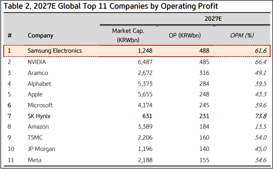
@MikeFritzell I don’t think it’s completely unreasonable. It’s a somewhat dated estimate, and you can just assume SK Hynix’s estimates have moved up since then.
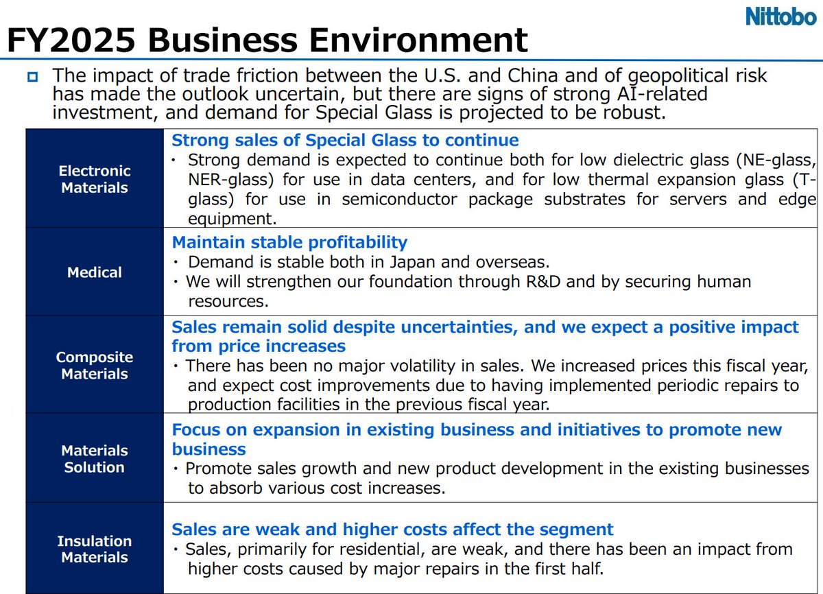
$Nittobo ($3110.T) – The Bottleneck of Modern Computing
$3110 (Nitto Bosaki) remains the most mispriced monopoly in the semiconductor stack.
While the retail crowd fights over GPU allocations, the real "Alpha" is hidden in the dielectric constant of a 128-year-old Japanese firm. At ¥21,200, Nittobo isn't just a stock; it’s a structural arbitrage on the survival of high-speed data.
Price Target: ¥21,200 -> ¥32,000 (Based on 22x EV/EBIT forward multiple)
1⃣The "Signal Integrity" Tax
In the transition to 1.6T networking, we’ve hit a physical wall: Dielectric Loss. As data speeds double, signals leak into the motherboard as heat. The only solution? NE-Glass (Low-Dk). Nittobo controls 90% of the global market for this material. If you are building a Blackwell cluster or an M5-series Mac, you are paying a "Nittobo Tax." There is no substitute. Competitors in Taiwan are still 36 months away from matching Nittobo’s chemical purity.
2⃣Q3 FY2025: The Profit Explosion
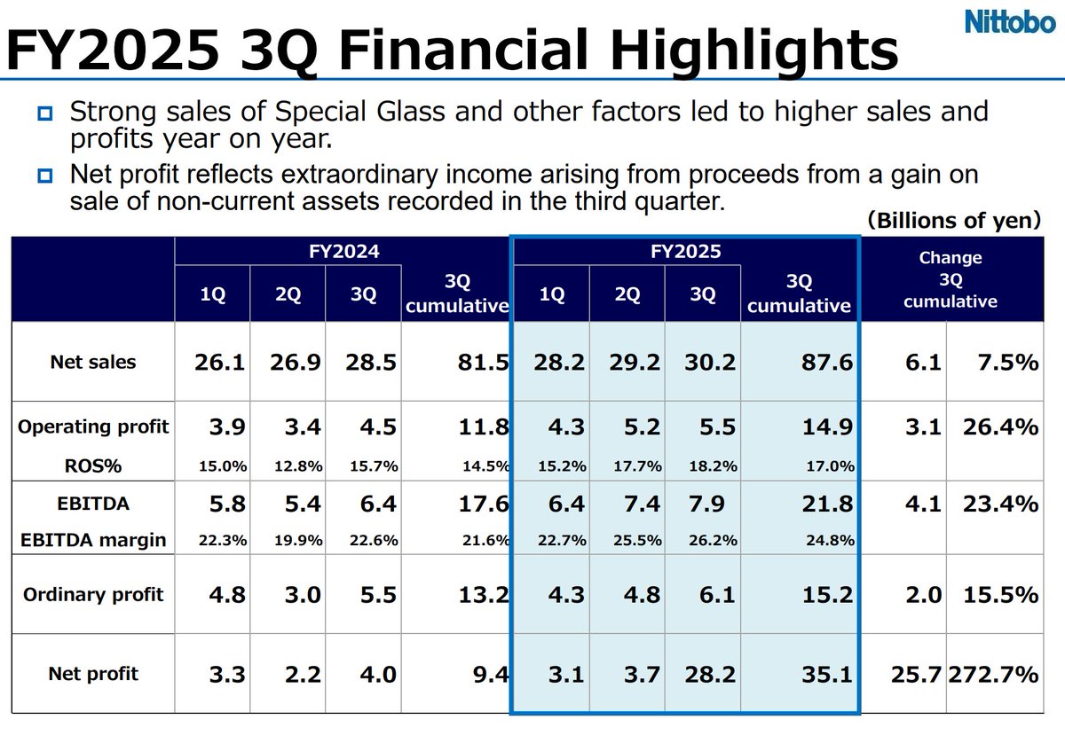
The latest February 2026 filings (Q3) aren't just good; they are anomalous.
Net Profit Surge: +272.7% YoY (¥35.1B).
Operating Leverage: While revenue in Electronic Materials grew 31%, segment profit exploded by 163.5%.
The Pivot: Nittobo has successfully cannibalized its low-margin construction business. They are now a pure-play tech enabler disguised as an industrial firm.
3⃣The "Apple vs. AI" Scarcity
The real "meat" for 2026 is the supply-demand mismatch. Nittobo’s order books for T-glass and NE-glass are effectively sold out through 2026. Apple is reportedly bypassing traditional supply chains to secure Nittobo’s production for the next iPhone generation. When a $3T titan like Apple fights for a Japanese manufacturer's capacity, "fair value" becomes a moving target.
4⃣NER-Glass: Leapfrogging the Competition
While the market prices in NE-Glass, Nittobo is already shipping NER-Glass.
The Moat: It reduces the thermal expansion coefficient by 30% (2.8ppm to 2.0ppm).
Why it matters: As AI chips get larger and hotter, they warp. NER-Glass is the only material that keeps the silicon flat. Nittobo has already locked in the 2027 standard while the competition is still trying to solve the 2024 problem.
5⃣The USD Play: Why Now?
For the USD investor, Nittobo at ¥21,200 is a rare Triple-Leverage Play:
Equity: A structural monopoly in the highest-growth tech sector.
FX: Acquiring an asset in historically cheap JPY.
Dividend: A record ¥114.00 forecast (30% payout). Management is finally returning the tech windfall to shareholders.
➡️Final Verdict⬅️
Nittobo is the "ASML of Glass."
It’s the invisible toll bridge of the AI era. At 20x forward P/E, it’s a bargain compared to US peers (Vertiv, Fabrinet) trading at 40x+.
The "Glass Ceiling" isn't just breaking; it’s being replaced by Nittobo’s NE-Glass.
Ticker: TYO: 3110 / OTC: NBCLF
Next Catalyst: FY2026 Full-Year Guidance (May).
When Apple starts fighting Nvidia for a Japanese glass-maker's capacity, you know the cycle has shifted from 'growth' to 'survival'.
I’ve laid out the data from the Q3 report, but I want to hear from you: Is Nittobo the ultimate 'pick and shovel' play, or is the JPY volatility too much of a hurdle for your USD portfolio? Let’s debate."
#Photonics #AI #Bottleneck #TSE #Nittobo #GlassSubstrate #Semiconductors